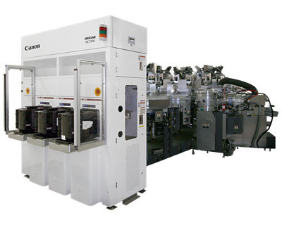
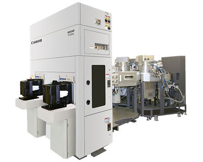
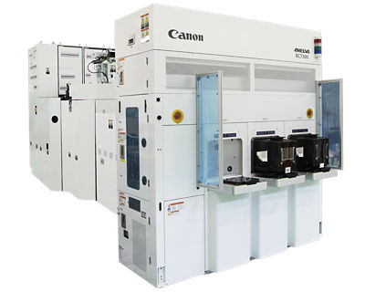
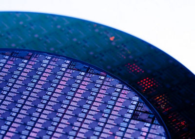
Canon Semiconductor Manufacturing Equipment is used in various industries, and we have a comprehensive line up of Front-End-of-Line (FEOL) and Back-End-of-Line (BEOL) equipment used for the semiconductor and display manufacturing processes.
Lithography
Canon's FPA (Fine Pattern Aligner) Series i-line, Deep Ultraviolet (DUV), and Nanoimprint Lithography systems are used in the fabrication and heterogeneous integration of high-tech displays and devices. These include light emitting diodes (LEDs), integrated circuits, image sensors, micro-electromechanical systems (MEMS), Radio Frequency (RF), photonic and power devices.
Deposition
Physical Vapor Deposition (PVD) plays a vital role in semiconductor and other industries. Our state-of-the-art technology allows you to deposit highly uniform films of thicknesses ranging from sub-nanometer to micrometers on wafers up to 300 mm diameter. Engineered to help you advance in your industry, this technology meets industry standards for low particle generation, high throughput, repeatability and cost-of-ownership.

Etch
Non-volatile Magnetic Random-Access Memory (MRAM) has a high potential for use in many high-end applications. Traditional etch processes, such as Reactive Ion Etch, are unable to satisfactorily etch the materials used in making MRAM, a common problem. To mitigate this issue, Canon has developed highly sophisticated etching equipment that uses an energetic beam of ions to etch the wafer in a controlled way.

Wafer Bonding
Existing and emerging applications like advanced packaging and power devices require permanent wafer bonding. Canon has developed equipment that uses Atomic Diffusion Bonding technology and is able to bond wafers at room temperature without application of high pressure. This not only makes the processing easier and faster but also enables new applications.

X-Ray Source
Non-destructive testing is becoming more and more important in the semiconductor industry, requiring an X-ray source capable of producing images with high resolution and at high speed. Canon has developed micro-focus X-ray sources capable of achieving resolution of 2 μm at 6 watts and 4 μm at 10 watts power, making them useful in applications such as X-ray microscopy, X-ray computed tomography and off-line non-destructive inspection.
Vacuum Components
Most semiconductor manufacturing processes are performed in a vacuum and the process equipment use a variety of vacuum components to create, measure and analyze vacuum. Canon manufactures high-quality vacuum components, such as pumps, gauges, leak detectors and mass spectrometers, vital for systems incorporating vacuum technology that include process equipment and measuring instruments.
Semiconductor Manufacturing Equipment and Industrial Products Catalog
Browse our catalog to view the entire list of products.


CONTACT US
Find contact information for specific departments for support, services, and product inquiries.

